Wednesday 12 November 2014

Minimizing the clock skew

the following is the technique should apply for minimizing the clock skew:

Buffering the clock:
In a large system, the single clock signal may not have adequate fanout to drive all of the devices, so it may be necessary to provide one or two copies of the clock signal.

Figure 1

The buffering method of figure1 produces excessive clock skew,
since CLOCK1 and CLOCK2 are delayed through an extra buffer compared to CLOCK
Figure 2


A recommended method is shown in figure 2.
all of the clock signals go through identical buffers and thus have roughly equal delays

Add delay in Data path:      
Figure 3

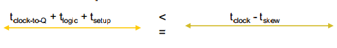
The amount of the inserted delay
(number of buffer and invters) in the data path should be large enough so that the delay becomes sufficiently greater than the clock skew.


Clock Reversing:

In this method, the clock signal arrives at the clock 
Figure 4
port of the destination register sonner than the
source register, so, the destination register will
clock in the source register ( current) value before the source register receives it's clock edge.


Alternate Phase Clocking:

the following are the most common methods of alternate phase clocking

  • clocking on alternate edges

In this method, the sequentially adjacent registers are clocked on opposite edges of the clock
this method provides a short path-clock skew margin of about one-half clock cycle.


  • clocking with two phases

In this method, the sequentially adjacent registers are alternatively clocked on two different registers,
there is a safety margin approximately equal to the phase difference of the two phases


Cmos Latch -up

Latch up is a functional chip failure associated with excessive current going through the chip, caused by weak circuit design.
the following diagram is drawing of a typical CMOS circuit. Notice the two transistors, NPN and PNP and their connection to VDD and GND supply rails. the two transistors are protected by resistors but if SCR device that could possibly be triggered.
Latch-up in CMOS


In a latch-up conduction the current flows from VDD to GND directly via the two transistors, causing the dangerous condition of a short circuit. the resistors are bypassed and thus excessive current flows from VDD to GND

Saturday 11 October 2014

SDC (Synopsys Design Constraints)

The rules that are written are referred to as constraints and  are essential to meet designs goal in terms of Area, Timing and Power to obtain the best possible implementation of a circuit.

There is a common format, for constraining the design, which is supported by almost all the tools, and this format is called SDC - Synopsis Design Constraints format.

The file is saved with an .sdc extention
SDC syntax is a TCL based format, that is, all commands follow the TCL syntax

SDC contains mainly following constraints that are very essential for design
  • Clock definition
  • Generated clock
  • Input/Output delay
  • Min/Max delay
  • False path
  • Multi cycle path
  • Case analysis
  • Disable timing arcs
The constraints are the following types according the commands types:
  • Basic commands
  • Object Access Commands
  • Timing Commands
  • Environment Commands
  • Multi-Voltage Commands

Basic Constraints commands
these commands used to set the attributes from that instance
cmd:    set: used to define variables
for example: set_units [-capacitance cap_unit] [-resistance res_units]
                                     [-time time_unit] [-voltage voltage_unit]
                                     [-current current_unit] [-power power_unit]

Object Access Constraints commands
These commands specify how to access objects in a design instance.
these commands are used to get the location of an object in the design.
the object can be a cell, a block, a port, a pin, or anything else in the design.
for example: 
      all_clocks
      # Returns a collection of all clocks.
      Examples:
      foreach_in_collection clkvar [all_clocks] {
       . . .}

      set_clock_transition 0.150 [all_clocks]

      get_libs [-regexp] [-nocase] patterns
      # Returns a collection of libraries that are currently
      # loaded in the design.


Timing Constraints commands
these commands are related to timing specifications of the design
which contains,
  • Clock definition          : create_clock
  • Generated clock          : create_generated_clock
  • Clock transition          : set_clock_transition
  • Clock Uncertainty      : set_clock_uncertainty 
  • Clock Latency            : set_clock_latency 
  • Propagated clock        : set_propagated_clock
  • Disable timing            : set_disable_timing
  • False path                   : set_false_path                     
  • Input/Output delay     : set_input_delay & set_output_delay
  • Min/Max delay           : set_min_delay / set_max_delay
  • Multicycle path          : set_multicycle_path
Environmental constraints
these commands are used to setup the environment of the design under analysis
commands are:
set_driving_cell
set_input_transition
set_load
set_max_fanout
set_max_area
set_operating_conditions
set_wire_load_model
set_case_analysis.......etc

Multi-Voltage Commands
these commands apply when multi-voltage islands are present in s design.
commands are:
create_voltage_area
set_level_shifter_strategy
set_level_shifter_threshold
set_max_dynamic_power
set_max_leakage_power

Friday 10 October 2014

Clock

Design includes the following types of Clock information:
  • Multiple clocks:
we can define multiple clocks that have different waveforms and frequencies. 
Clocks can have real sources(ports and pins) or can be virtual( no real source) in the design.
  • Gated clock


A gated clock is a clock signal 
under the control of the gating logic


  • Generated Clocks
A generated clock is a clock signal generated from another clock signal by a circuit within the design itself, such as a clock divider


  • Clock Transition times
 the transition time is the amount of time it takes for the signal to change from one logic state to anoher
  • Clock network delay and skew:
we specify the delay of the clock network relative to the source called clock latency  and
the variation of the arrival times of the clock at the destination points in the clock network called clock skew
  • Clock Latency: it can be ideal or propagated clocks
it has two types 1). Source Latency 2). Network Latency

Source latency is the delay between the ideal waveform to the source pin or port.
Network latency is the delay between the source pin or port to register clock pin 

If we specify the clock as propagated than PT can automatically compute the clock source latency
If not than user specified value is consider for clock source latency

Fig: External Source Latency


Propagated latency calculation is usually inaccurate for prelayout design because the parasitics are unknown.
For prelayout designs, you can estimate the latency of each clock and directly set that estimation with the
set_clock_latency command and it is known as ideal clocking

To specify an external uncertainty for source latency,
use the -early  and -late options of the set_clock_latency command.

For example, consider a source latency that can vary from 1.5 to 2.5ns as shown in above fig.
to specify this type of source latency, you can use commands such as following:

pt_shell> set_clock_latency 1.5 -source -early [get_clocks CLK]
pt_shell> set_clock_latency 2.5 -source -early [get_clocks CLK]

For Setup analysis, it uses the late value for each startpoint and the early value for each endpoint.
For hold analysis, it uses the early value for each startpoint and the late value for each endpoint.

Fig: Early/Late Source Latency waveforms


The following examples demonstrate how to set different source latency values for rising and falling edges.
To set the expected rise latency to 1.2 and the fall latency to 0.9 for CLK, enter
pt_shell> set_clock_latency -rise 1.2 [get_clocks CLK]
pt_shell> set_clock_latency -fall 0.9 [get_clocks CLK]

To specify an early rise and fall source latency of 0.8 and a late rise and fall source latency of 0.9 for CLK1, enter

pt_shell> set_clock_latency 0.8 -source -early [get_clocks CLK1]
pt_shell> set_clock_latency 0.9 -source -late [get_clocks CLK1]
Clock Uncertainty

Uncertainty = Skew + Jitter + margin

Clock Skew

Clock skew is a phenomenon in synchronous circuits in which the clock signal (sent from the clock circuit or source or clock definition point) arrives at different components at different times.
due to
  • wire-interconnect length
  • temperature variations
  • capacitive coupling
  • material imperfections and
  • differences in input capacitance on the clock inputs 
these factor became more critical for high frequency

Figure: Clock Skew 


there are two types of clock skew
  • Negative skew
  • positive skew
Positive skew occurs when the transmitting register receives the clock tick earlier than the receiving register.
Negative skew is occurs when the receiving register gets the clock tick earlier than the sending reg

Zero clock skew refers to the arrival of the clock tick simultaneously at transmitting and receiving reg

Skew can be caused two types of violation
  • Setup violation 
  • Hold violation

When the clock travels slower than the path form the one reg to another allowing data to penetrate two registers in the same clock tick, or maybe destroying the integrity of the latched data. this is called hold violation because the previous data is not held long enough at the destination flop to be properly clocked though.

if the destination flop receives the clock tick earlier than the source flop- the data signal has that much less time to reach the destination flop before the next clock tick, if it is fails to do so,a setup violation occurs, so called new data was not set up and stable before the next clock tick arrived.

Useful Skew
clock skew can also benefit a circuit by decreasing the clock period locally at which the circuit will operate correctly, it means skew add more margin to meet setup. that is called useful skew

for each source register and destination register connected by a path. so, following setup and hold inequalities must be obeyed.

for setup,
               T(clock period)  > = T(reg) + Path dealy(max) + J(jitter) + S(setup time) - Skew
for Hold,
               Skew <= T(reg) + Path delay(min) - J(jitter) - H(hold time)

Positive skews are good for fixing setup violation, but can cause hold violation
Negative skew can help hold violation, but can cause setup violation

Figure :1
Figure 1 show a situation where clock skew can benefit a synchronous circuit
In the zero skew circuit, a long path goes form FF1 to FF2, and short path, from FF2 to FF3,

here, Path FF2 -> FF3 path is close to having a hold violation: if small amount of extra clock delay occurs at FF3, this could destroy the data at D input of FF3 before clock arrives.
Figure 2
Figure 2 shows how the problem can be fixed
for clock skew.
A small amount of extra delay is added before FF2's clock input. with the care the extra delay relaxes the setup constraint for the FF1->FF2
here, for FF1->FF2 operates less than what required for zero skew.
so, some intentional skew helps in proper functioning of circuit,

NOTE: in above example, circuit is closer to malfunctioning- a small amount of positive clock skew for the FF2-> FF3 pair will cause hold violation, whereas the intentional skew(useful skew) circuit helps to meet the setup and hold constraints

Logic Synthesis

Which method would you use to design the logic circuitry for a million gate design?
I think we can use 
  • Paper & pencil : but it takes lots of month of time
  • Pspice schematic : it takes few month 
  • Logic Synthesis: it take very few days
so, Logic synthesis is the method of design which convert the RTL which is in the form of code, can convert to gates level design, which reduced the the ASIC design cycle dramatically.

Logic Synthesis
It is a process by which an abstract form of desired circuit behavior, typically at register transfer level (RTL), is turned into a design implementation in terms of logic gate

so, It is the process of Translating, Optimizing and Mapping 

PD interview Questiona - STA

What is crosstalk? What is the effect of crosstalk on timing? How to minimize crosstalk?


Crosstalk is phenomenon in which switching on a signal net effects switching activity of a nearby net due to capacitive coupling between two nets. Due to process-technology scaling, the spacing between adjacent interconnect wires keeps shrinking, which leads to an increase in the amount of coupling capacitance between interconnect wires. Hence, increase in the crosstalk effect. Crosstalk can severely effect timing in VLSI circuits. 
Cross-talk has two effects. 

1.Crosstalk delay 
2. Crosstalk noise

If if two adjacent wires are switching in opposite direction it will slow down signal hence violating set up time. 
If two net are switching in same direction it will aid timing. This is called crosstalk delay.This is random phenomenon. It depends on switching. 

If one net is switching and other is at constant value. The switching one net can cause induce voltage spike on other net. This is called crosstalk noise.

Methods for minimizing crosstalk:
1. Shielding of victim net by VDD/VSS line.
2. Upsize driver of victim net or downsize driver of aggressor net.
3. Add buffer on victim net.
4. Increase spacing between two nets.

PD interview Questions - Routing

1. What is the basic difference between 9 track and 12 track in standard cells? Who does a track means?

Firstly track can be related to lanes, eg like we say 6 lane road, implies 6 vehicles can run in parallel. So 10 tracks would imply we can route 10 wires in parallel with minimum pitch.

Now, 9/12 track implies 9 routing tracks are available for routing 9 wires in parallel with minimum pitch. For example if for 28nm we are using 9 track standard cell library with minimum metal pitch of 100n. In this case we will have standard cell of height 0.9um (100n*9) where 9 horizontal tracks are available for routing.

2. Why do we use alternate layer horizontal/vertical/horizontal (HVH or VHV) routing?

Some advantages of VHV/HVH:
To make best utilization of placement and routing resources.
To nullify crosstalk from layer beneath and above the routing layer.
More uniform distribution of power.

Why hold is independent of frequency?

Physical Design world have one critical problem that
if chip have setup violation than we can compromise on the chip performance and we can make chip to work on the lower frequency that it is design

But if chip have Hold violation than one question will arise in mind 
             'Will it work if we change the frequency ?'

than answer is no, because hold time is independent of frequency.
so, if we find hold violation after the chip design, than it is waste of effort


Fig: Setup time and Hold time is meet in the following figure

As shown in figure, in the window of Tsetup and Thold, data must remain stable. 


 Fig: Hold violation

Figure explain that there is hold violation due to data change in the Thold timing window which result into hold violation.


Now, one solution comes in mind,
'Can we fix the hold violation by reducing the frequency ?' 

The Answer is no.

Now, Lets understand the concept of why hold is free from the frequency?
(means changing the frequency cant fix the hold violation)

According to hold violation definition, data should remain stable after the active edge of clock for some minimum time

Fig: see the following figure that data is traveling from one ff1 to ff2

data1 = data at ff1
data2 = data at ff2
clock1= launch clock
clock2= capture clock


At the clock1, data1 is being sampled at ff2, and at clock2 data2( data of ff1 that is data1) is already reach to ff2 already

from the figure setup checks equation , that is
Tc2q(ff1) + Tcomb = Tclk - Tsetup
data1 of ff1 at clock1 should reach at ff2 in clock2 before the setup time of ff2.

from the hold checks,that is Tc2q + Tcomb >= T(hold)
data1 should not arrive at ff2 at clock2 before hold time because it override the data2.

which means that data is overridden by next data because data comes to much fast that override the previous data that is captured by previous clock edge, so, functionality of chip is getting failed.

If  the delay of combo logic and Tc2q delay is less than the hold time of ff2 than data comes too much fast that which does not give setup violation but result in hold violation, so, due to this condition data that is already capture data at ff2(data2) overrides by the data1 at the clock2 edge.
 so, it is only depends on the Tcombo and Tc2q, and Tcombo and Tc2q is not depends upon the clock period or working frequency.

so, Hold is independent of frequency.

Thursday 18 September 2014

What is the difference between a latch and a flip-flop?

Both latches and flip-flops are circuit elements whose output depends not only on the
present inputs, but also on previous inputs and outputs.

  • They both are hence referred as "sequential" elements.
  • In electronics, a latch, is a kind of bistable multi vibrator, an electronic circuit which has two stable states and thereby can store one bit of of information. Today the word is mainly used for simple transparent storage elements, while slightly more advanced  non-transparent (or clocked) devices are described as flip-flops. Informally, as this distinction is quite new, the two words are sometimes used interchangeably. [wiki] 
  • In digital circuits, a flip-flop is a kind of bistable multi vibrator, an electronic circuit which has two stable states and thereby is capable of serving as one bit of memory. 
  • Today, the term flip-flop has come to generally denote non-transparent (clocked or edge-triggered) devices, while the simpler transparent ones are often referred to as latches.[wiki]
  • A flip-flop is controlled by (usually) one or two control signals and/or a gate or clock signal. 
  • Latches are level sensitive i.e. the output captures the input when the clock signal is high, so as long as the clock is logic 1, the output can change if the input also changes.
  • Flip-Flops are edge sensitive i.e. flip flop will store the input only when there is a rising or falling edge of the clock. 
  • A positive level latch is transparent to the positive level(enable), and it latches the final input before it is changing its level(i.e. before enable goes to '0' or before the clock goes to -ve level.)
  • A positive edge flop will have its output effective when the clock input changes from '0' to '1' state ('1' to '0' for negative edge flop) only. 
  • Latches are faster, flip flops are slower.
  • Latch is sensitive to glitches on enable pin, whereas flip-flop is immune to glitches.
  • Latches take less gates (less power) to implement than flip-flops.
  • D-FF is built from two latches. They are in master slave configuration.
  • Latch may be clocked or clock less. But flip flop is always clocked.
  • For a transparent latch generally D to Q propagation delay is considered while for a flop clock to Q and setup and hold time are very important.

Cells Types in PD

In Physical Design flow, there are various kinds of cells used for several functionality. Each individual cells has there own functionality with which they are implemented in design. Here are some of the list of cells and their basic importance.


Spare Cells

When the design is tape-out and afterwards there is a requirement to fix some bug then it is not possible to fix if we haven’t provided spare cells. These are kind of floating cells which are thrown in design so that after tape-out if some bugs are needed to fix, we can take use of it.There would be inclusion of approximately 5% of spare cells in the whole design, not more than that.


Decap Cells 

They are temporary capacitors which are added in the design between power and ground rails to counter the functional failure due to dynamic IR drop. Dynamic IR Drop happens at the active edge of the clock at which a high current is drawn from the power grid for a small duration. If power source is far from a flop the chances are there that flop can go into metastable state. To overcome decaps are added, when current requirement is high this decaps discharge and provide boost to the power grid.

Detailed Discussion:http://www.cadence.com/Community/forums/p/11345/17149.aspx


Tie Cells

Tie-high and Tie-Low cells are used to connect the gate of the transistor to either power or ground. In Lower technology nodes, if the gate is connected to power/ground the transistor might be turned on/off due to power or ground bounce. These cells are part of standard-cell library. The cells which require Vdd (Typically constant signals tied to 1) connect to Tie high cells The cells which require Vss/Gnd (Typically constant signals tied to 0) connect to Tie Low cells.

For more details:

http://www.cadence.com/Community/forums/p/12129/16444.aspx


Well taps (Tap Cells)


They are traditionally used so that Vdd or GND are connected to substrate or n-well respectively. This is to help tie Vdd and GND which results in lesser drift and prevention from latchup.End cap Cells: The library cells do not have cell connectivity as they are only connected to power and ground rails, thus to ensure that gaps do not occur between well and implant layer and to prevent the DRC violations by satisfying well tie-off requirements for core rows we use end-cap cells.


Filler cells

Filler cells are used to establish the continuity of the N- well and the implant layers on the standard cell rows, some of the small cells also don’t have the bulk connection (substrate connection) because of their small size (thin cells). In those cases, the abutment of cells through inserting filler cells can connect those substrates of small cells to the power/ground nets. i.e. those thin cells can use the bulk connection of the other cells (this is one of the reason why you get stand alone LVS check failed on some cells).

PD Interview Questions - How does DFT logic affect PD ?

1. How does mbist logic affect placement ? Will knowing the algorithms used to assign controllers help in floorplan ? How does scan chain affect PD ?


MBIST (Memory built-in self-test) logic is inserted to test the memories. It contains MBIST processor & wrapper around the memories. MBIST processor controls the wrapper & generates various control signals during the memory testing. A single block may have multiple processors depending on the number of memories, memory size, power and memory placement. Memory placed nearby are grouped together & controlled by a single processor. 
Memory placement information needs to be given to the DFT team in form of DEF & floorplan snapshot (optional). 
If memories are not grouped properly according to their physical location i.e memories under same processors are sitting far apart. This will lead to MBIST logic spreading. 
This may have impact on MBIST timing due to long paths or increase in congestion due to lots of criss-cross.


2. what you mean by Scan Chain Reordering?

click on link for more information
http://vlsibasic.blogspot.in/2014/09/scan-chain-reordering.html

Scan Chain Reordering

It is the process of reconnecting the scan chains in a design to optimize for routing by reordering the scan connection which improve timing and congestion.
Since logic synthesis arbitrarily connects the scan chain, we need to perform scan reorder after placement so that the scan chain routing will be optimal
Based on timing and congestion the tool optimally places standard cells. While doing so, if scan chains are detached, it can break the chain ordering (which is done by a scan insertion tool like DFT compiler from Synopsys) and can reorder to optimize it & it maintains the number of flops in a chain.
Physical Netlist is reordered based on placement
Reordered scan chain requires much less routing resources in the example design.

Congestion Effect:
During placement, the optimization may make the scan chain difficult to route due to congestion. Hence the tool will re-order the chain to reduce congestion.

Timing Effect:
This sometimes increases hold time problems in the chain. To overcome these buffers may have to be inserted into the scan path. It may not be able to maintain the scan chain length exactly. It cannot swap cell from different clock domains.
Because of scan chain reordering patterns generated earlier is of no use. But this is not a problem as ATPG can be redone by reading the new netlist.

PD Intervie Questions - Floorplanning


Tuesday 29 July 2014

What is Design Exchange Format (DEF)?

A specification for representing logical connectivity and physical layout of and integrated circuit in ASCII format

Example:  


A DEF file is used to describe all the physical aspects of a design, including 
- Die size
- Connectivity 
- Physical location of cells and macros on the chip. 

It contains floor-planning information such as 
- Standard cell rows, groups
- Placement and routing blockages
- Placement constraints
- Power domain boundaries. 

It also contains the physical representation for pins, signal routing, and power routing, including rings and stripes.

Friday 25 July 2014

CPPR (Common Path Pessimism Removal)


We  know that setup is always check for worst corner and Hold is always check for Best Corner.

In OCV Analysis mode, for worst corner ,while Setup Analysis data path have max delay and clock path have min dalay and for best corner while Hold Analysis data path have min delay and clock path have max delay if we go for pessimistic approach.

Now we know that ,
Setup slack = Required time - Arrival Time
or we can say,    
Setup slack = Min delay path - Max delay path
And,
Hold slack = Arrival Time - Required Time
or we can say,
Hold slack = Min delay path - Max delay path

For Pessimism no need of derating for late(Max delay path) in setup and early (Min delay path) in hold Analysis.

Means At Worst Corner no need of late (data path ) only early (clock path) derating factor require for setup because worst corner itself is late and at Best Corner no need of early (data path) only late
(clock path) derating factor require for hold because best corner it self is early. 


Thats why we always give derating for clock path only.

CPPR :-
Removing common clock buffer delay between launch path and capture path is CPPR. (comman path pessimism removal).
Lets discuss with real time scenario,
Lets 0.2ns is common clock buffer delay for launch path and capture path.


Setup analysis,  

 If we dont consider derating factor for setup timing analysis than our calculation
 of setup slack will be in this manner:-
 setup slack = min path(c.p + (capture path + 0.2) + cppr - setup) – max path((
               launch path + 0.2) + data path) 
 
 where cppr = 0  (means no need of cppr if we are not analyzing with ocv mode)
 
 delay 0.2 ns will be cancel from both side thats how we can ignore same buffer delay
 in both path and our equation will change to :- 
 
 setup slack = min path(c.p + capture path - setup) – max path((launch path 
               + data path)
 
 But Because of  OCV (On chip Variation) delay we have to consider derating factor 
 in our design.
 
 Lets For clock path, 20% derating factor , 
 
 And we know that no need of derating for late in setup analysis so we apply derate 
 only for early so derating 20% of 1 for early is 0.8, 
 
 late -> 1.0     early -> 0.8 
 
 setup slack = min path(c.p + capture path + cppr - setup) – max path(launch path 
               + data path)

 So clock buffer delay for Max delay path, 0.2 * 1.0(late derate) = 0.2
 and clock buffer delay for Min delay path, 0.2 * 0.8(early derate) = 0.16
 
 so we can see that because of derating factor same clock buffer delay which was
 0.2ns now 0.16ns for min path and 0.2ns for max path.
 
 For removing this differences we add cppr in min path or can subtract from max 
 path. Normally we see that Tool add cppr in required timing path(min path) in 
 setup analysis. 
 
 Cppr = 0.2-0.16 = 0.04 
 or 
 cppr = 0.2 * (1.0-0.8) = 0.04 
 
 setup slack = (c.p + (capture path + 0.16) + 0.04 - setup) – ((launch path
                  + 0.2) + data path)
 Result,
 
 setup slack = min path(c.p + capture path - setup) – max path(launch path + 
               data path)
 
Hold Analysis,
 
 Lets for clock path, 20% derating factor , 
 
 Again we know that no need of derating for early in hold analysis so we apply 
 derating of late only. So derating 20% of 1 for late will be 1.2, 
 
 early -> 1.0     late -> 1.2 
 
 Hold slack = Min delay path(launch path + data path) - max delay path(capture 
              path - cppr + hold)
 
 Again lets 0.2ns is common clock buffer delay for launch path and capture path. 
 
 So clock buffer delay for Min path,  0.2 * 1.0(early derate) = 0.20
and clock buffer delay for Max path, 0.2 * 1.2(late derate) = 0.24
 
 Again we can see that because of derating factor same clock buffer delay which
 was 0.2ns now 0.2ns for min path and 0.24ns for max path.
 
 So for removing this differences we add cppr in max path or can subtract from min 
 path. Normally we see that Tool subtract cppr in required timing path(max path) 
 in Hold analysis. 
 
 Cppr = 0.24 – 0.20 = 0.04 
 or 
 cppr = 0.2 * (1.2 – 1.0) = 0.04 
 
 hold slack =  Min delay path(launch path + 0.20) + data path) - max delay path(
               (capture path + 0.24) – 0.04 + hold)
Result,
 hold slack =  Min delay path(launch path + 0.20) + data path) - max delay path(
               (capture path + 0.24) – 0.04 + hold) 
 

Different level of Design

Fig: following is the flow of how design is processing in the one level to other level 


Figure shows that how one idea that is written in some code, that is converting into the physible chip.

Where,
System level
- It is the abstract algorithmic description of high level behavior which is written in higher level language like C and it does not contain any implementation details for timing or data

RTL level
- It is accurate model very close to the hardware implementation which is describe in bit level
- it contains sequential constructs like if-than-else, while loops...... to support the modeling of complex control flow. for example:

module mark1;
reg [31:0] m[0:8192];
reg [12:0] pc;
reg [31:0] acc;
reg[15:0] ir;
always
   begin
         ir = m[pc];
        if(ir[15:13] == 3b’000)
         pc = m[ir[12:0]];
        else if (ir[15:13] == 3’b010)
        acc = -m[ir[12:0]];
     ...
   end
endmodule

Gate level
- it is describes models function in Boolean logic using registers and gates
- various delay models for gates and wires is defined


Transistor level
- it is describe in the form of CMOS
- depending on the application function modeled as resistive switches or full differential equations for circuit simulations


Layout level
- transistor and wires are laid out as polygons in different technology layers such as  diffusion, ploy-silicon, metals etc.


Thursday 24 July 2014

Understanding Setup and Hold Violations in Digital System Design

Fig: Following the flipflop circuit where data is transfer from D1 to Q3

The flipflops shown are positive edge triggered, i.e. on the positive edge of the clock, they takes the value of the signal at its input and send it to the flipflop’s output after a small delay called the tclock-to-Q


Fig: Following the figure of the different condition of data signals

The flipflops do their job correctly only if the signal at their inputs does not change for some
time before the clock edge (tsetup) and some time after the clock edge (thold).

Fig: Followin figure shown how data should propagate

Time to propagate a valid (no violations) signal at D2, to D3, counting from the clock edge at Flipflop2, 
is invariably = tclock-to-Q + tlogic. 
And for Flipflop3 to latch it, this signal has to be maintained at D3 for tsetup time before the clock tree sends the next positive edge of the clock to Flipflop3.


Fig: Following figure shows the condition of setup violation


To prevent setup violations..........


Fig: Following figure shows that how data should propagate without hold violation


For D2 to be able to send its signal to Q2, it must be left unchanged for thold time after a clock edge. That is, during this time, a signal from D1 should not be able to race through the combinational logic Comb1 and make it to D2.

Fig: Following figure shows the condition of hold violation

Therefore, to make sure the signal is HELD properly at the input of Flipflop2 without the
input of the previous Flipflop (D1) racing through


To prevent from hold violations:

Sunday 20 July 2014

What are Timing Libraries?

A library file is made of not only a list of gates but also contain the following
  • Functional or Logical definitions of the each gates
  • Power, energy characteristics for each inputs of the gate
  • Timing characteristics for delay of the gate
  • Physical characteristics which represents the area and footprint of the gate
  • Same gate is define by the different characteristics with different attributes of area, timing and power

When this timing library is given as an input to a synthesis tool along with the RTL code which is in the behavioral form, it converts it into the structural design.

Synthesis can replace gates with other gates of the same footprint without affecting the functionality for meeting the constraints of the design