Latch up is a functional chip failure associated with excessive current going through the chip, caused by weak circuit design.
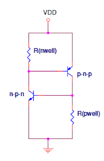
the following diagram is drawing of a typical CMOS circuit. Notice the two transistors, NPN and PNP and their connection to VDD and GND supply rails. the two transistors are protected by resistors but if SCR device that could possibly be triggered.
In a latch-up conduction the current flows from VDD to GND directly via the two transistors, causing the dangerous condition of a short circuit. the resistors are bypassed and thus excessive current flows from VDD to GND
the following diagram is drawing of a typical CMOS circuit. Notice the two transistors, NPN and PNP and their connection to VDD and GND supply rails. the two transistors are protected by resistors but if SCR device that could possibly be triggered.
 |
| Latch-up in CMOS |
In a latch-up conduction the current flows from VDD to GND directly via the two transistors, causing the dangerous condition of a short circuit. the resistors are bypassed and thus excessive current flows from VDD to GND


No comments:
Post a Comment