Tuesday 29 July 2014

What is Design Exchange Format (DEF)?

A specification for representing logical connectivity and physical layout of and integrated circuit in ASCII format

Example:  


A DEF file is used to describe all the physical aspects of a design, including 
- Die size
- Connectivity 
- Physical location of cells and macros on the chip. 

It contains floor-planning information such as 
- Standard cell rows, groups
- Placement and routing blockages
- Placement constraints
- Power domain boundaries. 

It also contains the physical representation for pins, signal routing, and power routing, including rings and stripes.

Friday 25 July 2014

CPPR (Common Path Pessimism Removal)


We  know that setup is always check for worst corner and Hold is always check for Best Corner.

In OCV Analysis mode, for worst corner ,while Setup Analysis data path have max delay and clock path have min dalay and for best corner while Hold Analysis data path have min delay and clock path have max delay if we go for pessimistic approach.

Now we know that ,
Setup slack = Required time - Arrival Time
or we can say,    
Setup slack = Min delay path - Max delay path
And,
Hold slack = Arrival Time - Required Time
or we can say,
Hold slack = Min delay path - Max delay path

For Pessimism no need of derating for late(Max delay path) in setup and early (Min delay path) in hold Analysis.

Means At Worst Corner no need of late (data path ) only early (clock path) derating factor require for setup because worst corner itself is late and at Best Corner no need of early (data path) only late
(clock path) derating factor require for hold because best corner it self is early. 


Thats why we always give derating for clock path only.

CPPR :-
Removing common clock buffer delay between launch path and capture path is CPPR. (comman path pessimism removal).
Lets discuss with real time scenario,
Lets 0.2ns is common clock buffer delay for launch path and capture path.


Setup analysis,  

 If we dont consider derating factor for setup timing analysis than our calculation
 of setup slack will be in this manner:-
 setup slack = min path(c.p + (capture path + 0.2) + cppr - setup) – max path((
               launch path + 0.2) + data path) 
 
 where cppr = 0  (means no need of cppr if we are not analyzing with ocv mode)
 
 delay 0.2 ns will be cancel from both side thats how we can ignore same buffer delay
 in both path and our equation will change to :- 
 
 setup slack = min path(c.p + capture path - setup) – max path((launch path 
               + data path)
 
 But Because of  OCV (On chip Variation) delay we have to consider derating factor 
 in our design.
 
 Lets For clock path, 20% derating factor , 
 
 And we know that no need of derating for late in setup analysis so we apply derate 
 only for early so derating 20% of 1 for early is 0.8, 
 
 late -> 1.0     early -> 0.8 
 
 setup slack = min path(c.p + capture path + cppr - setup) – max path(launch path 
               + data path)

 So clock buffer delay for Max delay path, 0.2 * 1.0(late derate) = 0.2
 and clock buffer delay for Min delay path, 0.2 * 0.8(early derate) = 0.16
 
 so we can see that because of derating factor same clock buffer delay which was
 0.2ns now 0.16ns for min path and 0.2ns for max path.
 
 For removing this differences we add cppr in min path or can subtract from max 
 path. Normally we see that Tool add cppr in required timing path(min path) in 
 setup analysis. 
 
 Cppr = 0.2-0.16 = 0.04 
 or 
 cppr = 0.2 * (1.0-0.8) = 0.04 
 
 setup slack = (c.p + (capture path + 0.16) + 0.04 - setup) – ((launch path
                  + 0.2) + data path)
 Result,
 
 setup slack = min path(c.p + capture path - setup) – max path(launch path + 
               data path)
 
Hold Analysis,
 
 Lets for clock path, 20% derating factor , 
 
 Again we know that no need of derating for early in hold analysis so we apply 
 derating of late only. So derating 20% of 1 for late will be 1.2, 
 
 early -> 1.0     late -> 1.2 
 
 Hold slack = Min delay path(launch path + data path) - max delay path(capture 
              path - cppr + hold)
 
 Again lets 0.2ns is common clock buffer delay for launch path and capture path. 
 
 So clock buffer delay for Min path,  0.2 * 1.0(early derate) = 0.20
and clock buffer delay for Max path, 0.2 * 1.2(late derate) = 0.24
 
 Again we can see that because of derating factor same clock buffer delay which
 was 0.2ns now 0.2ns for min path and 0.24ns for max path.
 
 So for removing this differences we add cppr in max path or can subtract from min 
 path. Normally we see that Tool subtract cppr in required timing path(max path) 
 in Hold analysis. 
 
 Cppr = 0.24 – 0.20 = 0.04 
 or 
 cppr = 0.2 * (1.2 – 1.0) = 0.04 
 
 hold slack =  Min delay path(launch path + 0.20) + data path) - max delay path(
               (capture path + 0.24) – 0.04 + hold)
Result,
 hold slack =  Min delay path(launch path + 0.20) + data path) - max delay path(
               (capture path + 0.24) – 0.04 + hold) 
 

Different level of Design

Fig: following is the flow of how design is processing in the one level to other level 


Figure shows that how one idea that is written in some code, that is converting into the physible chip.

Where,
System level
- It is the abstract algorithmic description of high level behavior which is written in higher level language like C and it does not contain any implementation details for timing or data

RTL level
- It is accurate model very close to the hardware implementation which is describe in bit level
- it contains sequential constructs like if-than-else, while loops...... to support the modeling of complex control flow. for example:

module mark1;
reg [31:0] m[0:8192];
reg [12:0] pc;
reg [31:0] acc;
reg[15:0] ir;
always
   begin
         ir = m[pc];
        if(ir[15:13] == 3b’000)
         pc = m[ir[12:0]];
        else if (ir[15:13] == 3’b010)
        acc = -m[ir[12:0]];
     ...
   end
endmodule

Gate level
- it is describes models function in Boolean logic using registers and gates
- various delay models for gates and wires is defined


Transistor level
- it is describe in the form of CMOS
- depending on the application function modeled as resistive switches or full differential equations for circuit simulations


Layout level
- transistor and wires are laid out as polygons in different technology layers such as  diffusion, ploy-silicon, metals etc.


Thursday 24 July 2014

Understanding Setup and Hold Violations in Digital System Design

Fig: Following the flipflop circuit where data is transfer from D1 to Q3

The flipflops shown are positive edge triggered, i.e. on the positive edge of the clock, they takes the value of the signal at its input and send it to the flipflop’s output after a small delay called the tclock-to-Q


Fig: Following the figure of the different condition of data signals

The flipflops do their job correctly only if the signal at their inputs does not change for some
time before the clock edge (tsetup) and some time after the clock edge (thold).

Fig: Followin figure shown how data should propagate

Time to propagate a valid (no violations) signal at D2, to D3, counting from the clock edge at Flipflop2, 
is invariably = tclock-to-Q + tlogic. 
And for Flipflop3 to latch it, this signal has to be maintained at D3 for tsetup time before the clock tree sends the next positive edge of the clock to Flipflop3.


Fig: Following figure shows the condition of setup violation


To prevent setup violations..........


Fig: Following figure shows that how data should propagate without hold violation


For D2 to be able to send its signal to Q2, it must be left unchanged for thold time after a clock edge. That is, during this time, a signal from D1 should not be able to race through the combinational logic Comb1 and make it to D2.

Fig: Following figure shows the condition of hold violation

Therefore, to make sure the signal is HELD properly at the input of Flipflop2 without the
input of the previous Flipflop (D1) racing through


To prevent from hold violations:

Sunday 20 July 2014

What are Timing Libraries?

A library file is made of not only a list of gates but also contain the following
  • Functional or Logical definitions of the each gates
  • Power, energy characteristics for each inputs of the gate
  • Timing characteristics for delay of the gate
  • Physical characteristics which represents the area and footprint of the gate
  • Same gate is define by the different characteristics with different attributes of area, timing and power

When this timing library is given as an input to a synthesis tool along with the RTL code which is in the behavioral form, it converts it into the structural design.

Synthesis can replace gates with other gates of the same footprint without affecting the functionality for meeting the constraints of the design

Library Timing characteristics

For delay calculation, this timing characteristics part is used which is in the form of lookup tables

Timing characteristics is defined in the multiple lookup tables for each type of delay that are
  • Rise delay
  • Rise transition 
  • Fall delay
Following is the example of timing characteristics

- lookup table contain two variables and the full  N x N lookup tabel is displayed, where N is positive integer

Example:
                    pin(Y) {
                    direction: output;
                    capacitance: 0.0;
                    function: "(A B)";
                    internal_power() {
                               related_pin: "A";
                               cell_rise(delay_template_7x7) {
                                            index_1 ("0.04, 0.07, 0.1, 0.2, 0.5, 1.0, 2");
                                            index_2 ("0.006, 0.030, 0.078, 0.174, 0.366, 0.749,1.523");
                                            values ( \
                                           "0.07, 0.09, 0.13, 0.20, 0.35, 0.64, 1.23", \
                                           "0.08, 0.10, 0.13, 0.21, 0.35, 0.65, 1.24", \
                                           "0.09, 0.11, 0.15, 0.22, 0.37, 0.66, 1.25", \
                                           "0.11, 0.13, 0.17, 0.25, 0.39, 0.68, 1.28", \
                                           "0.14, 0.17, 0.20, 0.28, 0.42, 0.72, 1.31", \
                                           "0.18, 0.21, 0.25, 0.33, 0.47, 0.76, 1.35", \
                                           "0.23, 0.26, 0.31, 0.39, 0.54, 0.83, 1.42");
                               }
( To understand the format of the lookup table, study the template of timing characteristics template in library)

Here,
index_1 represents input net transition and
index_2 represents total output net capacitance
depending on the various values for these indexes, corresponding delay values are looked up from the table
here, table can be any size 3 x 3, 7 x 7 etc depending upon the library vendor.
Now, how it work lets understand with the following example
here, 
- 7 x 7 indicates the size of the lookup table to be 7 rows and 7 columns
- index_1 indicates the factor for row indices 
- index_2 indicates the factor for column indices

what would the cell_rise time be if the input_net_transition is 0.1 and the total_ouptut net capacitance is 0.030?
answer : from the table, we get the value to be 0.11ps

Thursday 17 July 2014

How to Understand the Congestion Report in Design Compiler Graphical

I have a congestion report that includes the following information

Both Dirs: Overflow = 48090 Max = 15 (1 GRCs) GRCs = 47264 (0.18%)
H routing: Overflow = 26229 Max = 12 (1 GRCs) GRCs = 26149  (0.10%)
V routing: Overflow = 21861 Max = 4 (3 GRCs) GRCs = 21115  (0.08%)

The “Max” value in “Both Dirs” reports the largest total violation in both horizontal and vertical directions per global route cell.

The “Max” value in “H routing” reports the largest total violation in the horizontal direction, and
the “Max” value in “V routing” reports the largest total violation in the vertical direction.

For example,

if the cell that has the largest violation in the horizontal direction has a Max value of 12, and
it has a Max value of 3 in the vertical direction, the Max number in "Both Dirs" is 15.

The "GRCs" value is the total number of global routing cells with any violation.

The percentage (%) value is the percentage of global routing cells that have violations out of the total number of global routing cells in the design.


In the report you provided, there are 26,149 global routing cells that have violations in the horizontal direction and 21,115 global routing cells that have violations in the vertical direction.

The report for both directions indicates that 47,264 global routing cells have violations in the horizontal direction or the vertical direction.

What is "Clock Reconvergence Pessimism Removal" (CRPR)?

Clock reconvergence pessimism (CRP) is a difference in delay along the common part of the launching and capturing clock paths.

the most common causes of CRP are reconvergent paths in clock network, and different min and max delay of cells in the clock network.
CRP is an undesired effect.
clock reconvergence pessimism is an accuracy limitation of STA in general.
The inaccuracy occurs when the analysis tool compares two different clock paths that partially share a common physical path segment, and it assumes the shared segment has a minimum delay for one path and a maximum delay for the other path.
This condition can occur any time that launch and capture clock paths use different delays of reconvergent logic.
The two clock paths that feed into the multiplexer A cannot be active at the sametime, but an analysis could consider

Below is an example, both the shorter and longer paths for one setup or hold check, even without case analysis. 
Fig: below fig is the example of CRPR


pt_shell> set_operating_conditions -analysis_type \
               on_chip_variation -min MIN -max MAX
pt_shell> set_timing_derate -net -min 0.80 -max 1.00
here, command set up a variation analysis using a 20% derating that is performed at 100% worst case and then at 80% worse case and repeated for best case also.
The problem arises when the clock network diverges from the common segment, here in above example clock diverges from the U1, resulting in two path.
Now, using above PT command as mention, we are doing min/max analysis using On chip variation.
In the setup check, the second flip-flop,
path-1: clock path to source path ( CLK to LD1/cp) at the 100% worst case, and
path-2: clock path to destination path ( CLK to LD2/cp) at the 80% worst case
(this is because, while setup analysis data path have max delay and clock path have min delay)
This is valid approach beacuse test is pessimistic
here, path-1 and path-2 share a clock tree until the ouput of U1.
the setup check considers that cell U1 simultaneously has two different delays,
 min= 0.64 and max= 0.80
resulting in a pessimistic analysis delays in the amount of 0.16.

so, test is more pessimistic by 0.16 value and it must be remove for more realistic.
By default, the CRPR setting is false
To enable CRPR:
pt_shell> set timing_remove_clock_reconvergence_pessimism TRUE

Example timing report showing CRPR
****************************************
Report : timing
-path full
-delay max
-max_paths 1
Design : my_design
****************************************
Startpoint: LD1 (rising edge-triggered flip-flop clocked by CLK)
Endpoint: LD2 (rising edge-triggered flip-flop clocked by CLK)
Path Group: CLK
Path Type: max
Point Incr Path
---------------------------------------------------------------
clock CLK (rise edge)                                         0.00 0.00
clock network delay (propagated)                        1.40 1.40
LD1/CP (FD2)                                                    0.00 1.40 r
LD1/Q (FD2)                                                      0.60 2.00 f
U1/z (AN2)                                                         3.20 5.20 f
data arrival time                                                            5.20
clock CLK (rise edge)                                          6.00 6.00
clock network delay (propagated)                         1.16 7.16
clock reconvergence pessimism                        0.16 7.32
clock uncertainty                                                   0.00 7.32
LD2/CP (FD2)                                                             7.32 r
library setup time                                                 -0.20 7.12
data required time                                                         7.12
---------------------------------------------------------------
data required time                                                         7.12
data arrival time                                                           -5.20
---------------------------------------------------------------
slack (MET)                                                                 1.92

Wednesday 16 July 2014

Why setup/hold time come into picture for Reg?

                        Sequential Circuit Timing

This section covers several timing considerations encountered in the design of synchronous sequential circuits

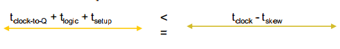
Why setup time and hold time arise in a flip flop?

To understand why setup and hold time arises in a flip-flop one needs to begin by looking at its basic function. 

These flip-flop building blocks include inverters and transmission gates.

    Fig: Inveter diagram
 Inverters are used to invert the input


Fig: Transmission gate (Tx)

It is a parallel connection of nMOS and pMOS with complementary inputs to both MOSFETs
It is Bidirectional, it carries current in either direction. Depending on the voltage on the gate, the connection between the input and output is either low-resistance or high-resistance, so that Ron = 100 Ω or less and 
Roff > 5 MΩ. This effectively isolates the output from the input.


The transistor level structure of a D flip-flop contains two 'back-to-back' inverters known as a 'latching circuit,' since it retains a logic value. Immediately after the D input, an inverter may or may not be present (see figure)

Fig The transistor level structure of D flip-flop contains two back-to-back inverters known as a'latching circuit.

The transistor level structure of D flip-flop contains two back-to-back inverters known as a'latching circuit.

It is a positive edge triggered flip flop because output arrives at the positive edge of clk

When clk = 0 , if D changes, the change would reflect only at node z 
When clk = 1,  it would appear at the output only 

Here, setup and hold time came into picture

Lets refresh what is setup and hold time?

Setup time: it is defined as the minimum amount of time before the clock's active edge that data must be stable for it to be latched correctly.

Hold time:  it is defined as the minimum amount of time after the clock's active edge during which data must be stable.

Here, setup and hold time is measured with respect to the active clock edge only.

why setup time came into picture?

see the following fig carefully


Fig: node D to Z delay is called setup time 
when D=0 and clk=0, 
input D is reflected at node z, so it take some time to reach the node z via path D-W-X-Y-Z.
The time that data D take to reach at node Z is called setup time

this defines the reason for the setup time within a flip flop.
so, it is necessary that data must be stable before the active edge of clock with delay value of the D to Z node of the latch unit of flip flop and this delay define the setup time of the register

Note: 
when the clock =0 , LHS part of the flop is active and RHS part is inactive due to clock is inverted in the RHS region
same, for when clock =1, LHS part of the flop is inactive and RHS part is active, and reflect the result of D input.

Fig: see the where is setup time came


Why Hold time came into picture?

here, flop is made of two latch unit with working in master and slave logic working fashion
so we can assume the LHS part is as Latch-1 and RHS part is as Latch-2

see fig carefully

Now, for working clk will always in invert in nature, so 
when latch-1 is active than latch -2 is inactive
when latch-2 is active than latch-1 is inactive

here, hold time came into picture
Time taken by the latch to come into active mode from inactive mode called hold time.
form this switching  hold time came
 or 
 we can also understand by this way that
there is the finite delay between the clk and clkbar, so transmission gate some time to switch on and off.
In meantime it is necessary to maintain a stable value at the input to ensure a stable value at node W, which in turn translates to the output, that defining the reason for the hold time within a flop.

there may be combo logic sitting before the first transmission gate ( here you can see the inverter before the transmission gate at the input path from D to W). This introduces a certain delay in the path of input data D to reach the transmission gate. this delay establishes whether the hold time is positive, negative or zero.

Now this relationship between the Combo logic delay and time taken for transmission gate to switch On and Off after clk and clkbar is given. that relationship between that rise to various types of hold time that exist, it can be +ve,-ve or zero hold time.

here, Tcombo define  the delay before first transmission gate
         Tx  define the time taken for transmission gate to switch on and off
         CLK represents the clock with an active rising edge
         D1, D2 and D3 represent various data signals
         S represents the setup margin
         H1, H2, and H3 denotes the respective hold margins

Fig: Hold time  due to Tx and Tcombo