Wednesday, 14 October 2015

MULTI BIT FLOP

Find flops that are placed close together and have the same clock and replaces them with Dual or multi-bit flops

CONCEPT
A 1-bit flip-flop has two latches (Master latch and slave latch). The latches need “Ck” and “Ck’ ” signal to perform operations.
In order  to  have  better  delay  from  Ck-> Q, we will regenerate “Ck” from “Ck'”. 

Hence we will have two inverters in the clock path.


Each 1-bit flip-flop contains two inverters, master-latch and slave-latch.Merging  single-bit  flip-flops into  one  multi-bit  flip-flop  can  avoid  duplicate  inverters,  and  lower  the  total clock dynamic power consumption.

REQUIREMENT
The single-bit flip-flops we want to replace with multi-bit flip-flop must have same clock and set/reset condition. 


STEPS TO FOLLOW
Below are few steps can follow or can make a script if want to use in design.

1)Find the flops that can be considered for replacing 
For example, all instances of following lib cells only can use for replacing.
{cell name : 1_bit_dff}
find for all the cells and than add them in array with name flops_for_mbit

2)Take first flop (lets name X)  from array flops_for_mbit to Check nearby flops to combine.
(a)first get x and y coordinate of first flop
(b)get Net driving to clk pin of that flop.
(c)find nearest instances  to that flop with some (for eg 5 micron) spacing in all  sides(left,right,bottom,top) 
 ex. locx->30 and locy ->70
-> give the address of all inst in [25 65 35 75 ] dimesion and sort them 
 After finding the flops in above dimension first,
->exclude near inst if same inst (X).
->exclude inst if not in flop_for_mbit array.

(d)Lets we found 2 near flops(lets name A,B) so we will take first near flop  (start with A) 
     and check net driving to clk and reset pin of that flop.
     (i)Now check to make sure that clocks(*/CK net)) and  (*/RESET net)  are same of first
         near inst A with first flop X.
     (ii) get distance from first flop X to first near flop A.

(e)Sort both near instances (A and B)  according to their distance from X in increasing
    order, we can give it a name as  sorted_flops.

(f)Now combine the closest instances into an mbit flop
     (i)find clk net,scan net of X flop CK,SCAN &RESET  pins which can be use for mbit flop 
         later so we will not take separate CK,SCAN & RESET pin for all flops which are using 
         in 1-bit flop.
     (ii)set cell Name but  need to check with library team that what should be the flop for 
          Multi Bit .
      lets we want to make 2-bit flop and it cell can be like lvt_2_bit_flop.
     (iii)set instname to new mbit flop for example MULTI_BIT_FLOP_0
     (iv)attach CK,SCAN and RESET net to MULTI_BIT_FLOP_0 instance CK ,SCAN and RESET              pin.
     (v)Now List all inst X to B first X and other according to sorted_flops.
          ->Take first flop X take its D pin  and Q pin net name(lets DN and QN) and attach
              with MULTI_BIT_FLOP_0 inst. 
             Since we want to use 2-bit flop As we need only 2 bit so we can give D as D0 and
             for next nearby inst it will be D1 and same for Q.
          ->Also take x,y coordinate of X flop which we add with all near flops x and y 
             coordinate and do avarege to get x,y coordinate of MULTI_BIT_FLOP_0.
          ->Delete X flop as its added in MULTI_BIT_FLOP _0 as not needed now.
     (vi) Now since total near flops are 2(A,B) and after adding our main flop(X) total 3 flops 
           but we need only two flops for 2-bit MBIT_FLOP so stop after count reach to 2 it can
           be (X,A) OR (X,B).
          Lets for example all flops which combine to make MBIT_FLOP_0 are (X,A).

So in the end INSTANCE MULTI_BIT_FLOP_0 WITH PINS CK,SCAN,RESET,DO,D1,Q0,Q1 and their respective nets attached with them also its coordinate will be  x= (x(X)+x(A))/ 2) and y = (y(X) + y(A))/2
For example,
X, (x,y) = 2,7
A, (x,y) =  2,8
Coordinate of MULTI_BIT_FLOP_0, (x,y) = (4/2, 15/2) = (2,7.5)

3)Revise step 2 for all remaining flops in flop_for_mbit array also next flop instance name will change to MULTI_BIT_FLOP_1 and continuous changing till last flop,
Note : We are deleting  flop once its used in MULTI_BIT_FLOP so it will not come in use for other MULTI_BIT_FLOP.

ADVANTAGES OF MBIT FLOPS:

1)Decrease total density of design and delay due to shared transistor.
2)Reduce total clock dynamic power consumption as less number of inverter or by avoiding duplicate inverter.
3)Also decrease number of hold buffer use for design.
4)Reduce clock skew in sequential gates.

DISADVANTAGES OF MBIT FLOPS;
Congestion can degrade as more pins on mbit flops which later increase shorts and drcs in design.

Tuesday, 8 September 2015

Fixing Hold

There are few ways we can fix hold without effecting setup violations ,

All data verified on 16nm design,

1) Swapping lower vt cells to higher vt is the best way to improve hold.

2) Also we can use delay cells if not able to improve hold through  vt swaping.
We need to go through a procedure if we want to fix hold in automated way.

a) first we need to take setup  slack limit on each and every pin of design and  finding pin with worst setup from all corner.
so now we have pins with worst setup so now we can fix hold by adding delay cells by finding setup margin of pin where we want to add delay cells.

b) Now we can find all timing paths on which hold is violated .

c) For different hold violation limit it will add different delay cells.

Hold slack,

limit 1   : -0.005
limit 2   : -0.015
limit 3  :  -0.035

Buffers can be used as : buf, 16_svt_delay25, 16_svt_delay50, 16_svt_ delay75


Data on setup margin limit for each buffer in different blocks,
 
        Buffer                                        delay after adding buffer          
16_svt_delay25                                  17ps - 89ps          
 Comment : For 4-5 cells its 137ps that because of long nets means high transition  as doing hold fix through script after functional Eco implementation.
16_svt_delay50                                  37ps - 112ps
16_svt_delay75 :                                53ps - 117ps

 hold slack limit                           setup margin                        buffers
 slack >  -0.05                                50ps                                16_lvt_sbuf
-0.005 <=slack>= --0.015               100ps                             16_svt_delay25
-0.015 <=slack>= --0.035               120ps                             16_svt_delay50
 slack < -0.035                              150ps                             16_svt_delay75


d) At last we can go through each path from endpoint to startpoint.and wherever we will find setup margin it will stop searching and  attach delay cell to that pin.

for being more pessimistic we can modify script to search for best margin in particular path and at that pin attach delay cell.

for ex. if we have to add delay25 cells we need margin of 100ps and we found 100ps margin at 1st level from endpoint to startpoint way but if we go little more ahead than we found margin of 150 ps which is best margin so script will attach delay cell to pin with 150ps margin.

Advantage with not searching for best margin that script will attach delay cell at  end  of  the path which can improve hold violations of other startpoints also for which this endpoint is common till that point.
So in the end it wilt help to add less delay cells for design compare to searching for best margin.

Comparison on adding delay cells for best margin and till limit,

 Total 80 paths which need to fix,
Starting from endpoint
With Best margin limit          :    Added 48 delay cells to fix hold completely
Starting from Endpoint
with Threshold limit              :    Added 43 delay cells to fix hold completely
Starting from startpoint
with Threshold limit              :    Added 44 delay cells to fix hold completely

3)If their is very less hold violation in design and we don't want to add delay cells or swap cells than we can reroute  or detour the net which will add some delay in path and fix the hold without effecting setup.

Min Pulse Width

Min pulse width check is to ensure that pulse width of  clock signal is more than required value. 

Basically it  is  based on frequency of operation and Technology.  Means if frequency of design  is 1Ghz than typical value of each high and low pulse width will be equal  to (1ns/2) 0.5ns if duty cycle is 50%.

Normally we see that in most of design duty cycle always keep 50% otherwise designer can face issues like clock distortion and if in our design  using half cycle path means data launch at +ve edge and capturing at -ve edge and again min pulse width as rise level and fall level will not be same and if lots of buffer and inverter will be in chain than it is possible that pulse can be completely vanish. 

Also we have to consider the best and worst case when clock get routed and depend on that decide that what should be the required value of Min Pulse Width. 

Now we know that  rise delay and fall delay of  combinational cells  are not equal so if a clock entering in a buffer than the output of clock pulse width will be separate to input.
So for example, if buffer rise delay is more than fall delay than output of clock pulse width for high level will be less than input.

so,  
High pulse : 0.5-0.056+ 0.049 = 0.493 & 
Low pulse :   0.5-0.049+0.056 = 0.507

For better understanding we go with real time scenario for Min Pulse Width.

Normally for clock path we use clock buffer because of the equal rise delay and fall delay of these buffer compare to normal buffer but this delay is not exact equal thatswhy we have to check min pulse width.

We can understand it with an example :-

Lets there is a clock signal which is going to clock pin of  flop through series of buffers with different rise and fall delay.  we can calculate  that how it effect to high or low pulse of clock.
we can  understand through calculation:-

High pulse width  = 0.5 + (0.049 - 0.056) + (0.034 – 0.039) + (0.023 –     0.026)  + (0.042 – 0.046) + (0.061 – 0.061) + (0.051 – 0.054) = 0.478ns

Low Pulse width = 0.5 + (0.056 – 0.049) + (0.038 – 0.034) + (0.026 – 0.023)  + (0.046 – 0.042) + (0.061 – 0.061) + (0.054 – 0.051) = 0.522ns

Lets required value of Min pulse width is 0.420ns.
Uncertainty =  80ps
than high pulse width = 0.478-0.080 = 0.398ns
Now we can see that we are getting violation for high pulse as total high pulse width is less than Require value.
So for solving this violation we can add an inverter which will change the transition and improve it.

Power Dissipation in CMOS

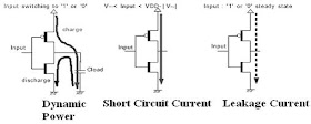
 There are three types of power dissipation in CMOS
1. Dynamic power is dissipated only when switching
2. Leakage current is permanent and results in a continuous loss
3. Short circuit

Ptotal = Pswitching + Pshort-circuit + PLeakage
Where,
Pswitching = CLoad  * (VDD ^2)  * f
Pshort-circuit = tsc * VDD * Isc 
PLeakage = VDD * Ileakage

Where, CLoad  = Capacitive loading due to pin and nets
             VDD = Supply Volatage
             tsc =  short circuit time in cmos
             Isc = short circuit current from pmos to nmos
             Ileakage = leakage current


where leakage power is also a funtion of Vdd, Vth and W/L ratio


Friday, 4 September 2015

Noise Margin

Noise margin is a parameter closely related to the input-output voltage characteristics. This parameter allows us to determine the allowable noise voltage on the input of a gate so that the output will not be affected. The specification most commonly used to specify noise margin (or noise immunity) is in terms of two parameters-
The LOW noise margin, NML, and the HIGH noised margin, NMH.
NML is defined as the difference in magnitude between the maximum LOW output voltage of the driving gate and the maximum input LOW voltage recognized by the driven gate. Thus,
NML (NOISE MARGIN low) = Vil - Vol

The value of NMH is difference in magnitude between the minimum HIHG output voltage of the driving gate and the minimum input HIGH voltage recognized by the receiving gate.Thus,
NMH (NOISE MARGIN high) = Voh - Vih

following to two figure hlep you to understand it better,


consider the following output characteristics of a CMOS inverter. Ideally, When input voltage is logic '0', output voltage is supposed to logic '1'. Hence Vil (V input low) is '0'V and Voh (V output high) is 'Vdd'V.
Vil = 0
Voh = Vdd 
Ideally, when input voltage is logic '1', output voltage is supposed to be at logic '0'. Hence, Vih (V input high) is 'Vdd', and Vol (V output low) is '0'V.
Vih = Vdd
Vol = 0 
Noise Margins could be defined as follows :
NML (NOISE MARGIN low) = Vil - Vol = 0 - 0 = 0
NMH (NOISE MARGIN high) = Voh - Vih = Vdd - Vdd = 0 

But due to voltage droop and ground bounce, Vih is usually slightly less than Vdd i.e. Vdd', whereas Vil is slightly higher that Vss i.e. Vss'. 
Hence Noise margins for a practical circuit is defined as follows : 

NML  (NOISE MARGIN low) = Vil - Vol = Vss' - 0 = Vss'
NMH (NOISE MARGIN high) = Voh - Vih = Vdd - Vdd' 

Following figure, explain about input and output characteristics of each transitors

Wednesday, 2 September 2015

Crosstalk

While chip designing, three factor that comes into picture
  • Power          : battery backup should be last longer
  • Performance: at same time, more than one application, each application have same working performance
  • Area             : same area, more more application can be installed
These three factor generate: Crosstalk

Let see one by one, crosstalk related topics

2. How Noise Margin come into picture of crosstalk
3. Crosstalk Glitch and factors affecting Glitch height
4. AC noise margin
5. Timing Windows, reasons for crosstalk
6. Impact of crosstalk on Setup and Hold timing
7. Techniques to overcame from crosstalk


Crosstalk Reasons

Reasons
1. High Density of standard cells
2. High Routing Density
Crosstalk comes into picture due to coupling capacitance, below figure may help you to understand the coupling capacitance,
so, we can deduce one direct reason of cross-talk is spacing
for same area, if density of standard cells is high than more cross-talk
if compare, 0.25um (older mobile chips) vs 0.1um below chips, have density difference due to functionality addition in latest chips, so, it has high density due to transistor size and more functionality which make transistor placement very near to other transistor

3. Increase in number of metal layers, increase lateral capacitance
In higher technology node like 0.25um and above,
metal cross section area = w * t
where, w = metal net width and t = metal net thickness
so, At higher node technology, standard cells placed far apart form each other cells, and have enough space for routing, so, routing is possible on same metal area.
here, due to higher width of metal, inter layer capacitance became more n more dominant factor

while in lower node, for same area, number of standards cell increase, but routing method cant be same as higher node, due to higher complexity, routing cant be on same layer. and in other side, metal net width is also less, so, effective inter layer capacitance is not dominant
but, lateral capacitance comes into picture, as net routes very near to each others, and complexity is also high so, number of net routing is also very high, due to that at lower node lateral capacitance is major parasitic s while designing chips

4. Supply voltage
..will be updated soon


Saturday, 22 August 2015

How to decide on minimum spaceing between two macros?

The formula to calculate spacing between two macro is 

=  (width+spacing x number of pins /vertical routing layers) + spacing

It is better adding an additional spacing because you can avoid violation with the side of macros.

Wednesday, 4 March 2015

Die Size Estimation

Technology Inputs:
Gate Density per sq. mm = D
Number of Horizontal Layers = H
Number of Vertical Layers = V

Design Inputs:
Gate count (excluding memories, macros & subchips) = G
IO area, in sq. mm = I
Memory + Macros + Subchips area, in sq.mm = M
Target Utilization, in percentage = U %
Additional gate count for CTS, timing closure etc, in percentage = T %
Additional gate count for ECOs, in percentage = E %

Die area calculation:

Die Area in sq.mm = {[(Gate count + Additional gate count for CTS & ECO) / Gate density] + IO                                           area + Mem, Macro area} / Target utilization

Die Area = {[(G + T + E) / D] + I + M} / U


Aspect ratio, width, height calculation:

Aspect Ratio
                                 AR = width / height
                                       = Number of horizontal resources / Number of vertical resources
                                 AR = H / V

Height
                AR = W / H
                 W = H * AR ----- (1)
           
             Area = W * H
                     = H * H * AR (Expressing W in terms of H from (1)
                H2 = Area / AR
                 H = SQRT (Die Area / AR)

Width

                W = H * AR


Aspect ratio is defined as the ratio of height to width